网站首页 公司简介 新闻动态 诚聘英才 联系我们  
产品系列
科研级光谱测试系统
科学级成像相机
真空紫外光谱测试
表面分析测试系统
FLIM 系统
激光器和光源
时间控制系统
耗材材料
光束整形元件
特种镜头
光学平台
光机配件
光镊微操控系统
光学元件检测与装调设备
激光直写系统
系统方案设计与服务
教学演示仪器
栏目列表
新闻动态
公司产品
服务与支持
当前位置: 首页 > 公司产品 > 激光直写系统 >

掩膜板制作与检测系统

作者: Kevin Peng    发布于: 2015-03-24 23:52    点击:
Precision pattern generators  掩膜板激光直写系统


Pattern generators are considered to be the most complex devices in mask making. High requirements for such equipment are met only with the help of high-end technology.
Scanning laser generators represent a new generation of multichannel laser pattern generators for making masks, reticles and direct writing on wafers without any die size limitation. The pattern generator enables to make high precision features on the mask, to write phase shift masks and optical proximity masks. Pattern generation time depends on die size only and is irrespective of the layer pattern complexity.


Production from 2012 7th generation: 90 nm technology node EМ-5389 Rmin=200 nm 
Production from 2008 6th generation: 180 nm technology node EМ-5289 Rmin=350 nm 
Production from 2005 5th generation: 350 nm technology node EМ-5189 Rmin=600 nm
Production from 1999 4th generation: 500 nm technology node EМ-5089B Rmin=800 nm
Production from 1994 3rd generation: 1.0 µm technology node EМ-5089A Rmin=1.0 µm
Production from 1988 2nd generation: 1.5 µm technology node EМ-5089 Rmin=1.5 µm
Production from 1988 1st generation: 2.0 µm technology node EМ-589B Rmin=2.0 µm


EМ-5389 Multichannel laser pattern generator

EМ-5289 Multichannel laser pattern generator

EМ-5189-01 Multichannel laser pattern generator


Special application pattern generator   特殊用途激光直写系统


A separate model line of laser pattern generators was developed by KBTEM-OMO for special applications in the semiconductor production.
Pattern generation is based on the microphotosetting principle.

EМ-5109 Laser pattern generator

 
Automatic mask inspection 全自动掩膜板检测系统 


Pattern inspection is of decisive significance in the semiconductor industry. Single microscopes as well as powerful optical systems are used for submicron structures. KBTEM-OMO developed a model line of systems for the automatic inspection of reticle patterns. Creation of the systems for the 45-60 nm technological node was a response to meet newest requirements of modern time.


Production from 2009 7th generation: 65-45 nm technology node EМ-6729   Rmin=65 nm
Production from 2008 6th generation: 110 nm technology node EМ-6329B   Rmin=150 nm
Production from 2006 5th generation: 180 nm technology node EМ-6329R  Rmin=250 nm
Production from 2001 4th generation: 350 nm technology node EМ-6029B Rmin=500 nm
Production from 1995 3rd generation: 800 nm technology node EМ-6029АМ Rmin=800 nm
Production from 1991 2nd generation: 1.0 µm technology node EМ-6029А Rmin=1.0 µm
Production from 1987 1st generation: 1.5 µm technology node EМ-6029 Rmin=1.5 µm


Laser-based mask defect repair systems  掩膜板缺陷激光修复系统

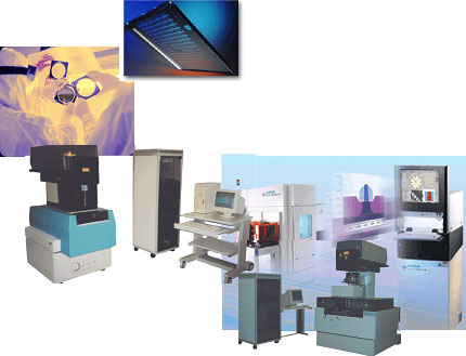
The laser-based mask defect repair systems are intended to repair photomasks with transparent and opaque defects.
A contour-projection method is used to form an optical image for the repair of opaque defects. Transparent defects are repaired through the laser-stimulated vapor deposition of metal-organic compounds.
Defects are detected automatically on the bases of the defect file formed at the inspection stage.
The model line of the laser-based mask defect repair systems, developed and manufactured by the company, is presented in the table as follows:

Production from 2009 6th generation: 90 nm technology node EМ-5131 Rmin=200 nm 
Production from 2007 5th generation: 180 nm technology node EМ-5201 Rmin=500 nm 
Production from 2001 4th generation: 350 nm technology node EМ-5001В Rmin=500 nm
Production from 1995 3th generation: 500 nm technology node EМ-5001AM Rmin=1.1 µm
Production from 1990 2rd generation: 1.0 µm technology node EМ-5001A Rmin=1.5 µm
Production from 1990 1nd generation: 1.5 µm technology node EМ-551B Rmin=2.0 µm


EМ-5131 Laser-based mask defect repair system

EМ-5001В Laser-based mask defect repair system


Systems for inspection of work masks   掩膜板在线检测系统

This class of equipment is intended for inspection of multiple work masks on the basis of master masks for series and low batch semiconductor production:
- Automated microsize inspection tool
- Mask pattern coordinates measurement system


Photorepeaters  光刻机 
 
  This class of equipment is intended for fabrication and inspection of step-and-repeat work masks on the basis of reticles for large-scale and low volume semiconductor production:
A contact printing system for patterning of work masks /under development/.
EМ-5062M Photorepeater


|关于我们|联系方式|客户留言|服务与支持|相关知识|友情链接|
Copyright © 2013-2019 FredorScience. 弗锐达科技 版权所有 沪ICP备13044418号-1